The subject of interest in this article is the company Nvidia and its collaboration with Samsung's 12-layer HBM3E chips. There could yet be some rare and precious external blessings from the Almighty that the Samsung HBM3E chips, based on 12-layer technology. This is so as the demands on AI and HPC towards a more general acceptance appear to be growing in the mid- to long-term, putting quite a few cartloads of limelight on advanced memory technology.

The Applications of HBM3E chips-What Are They?
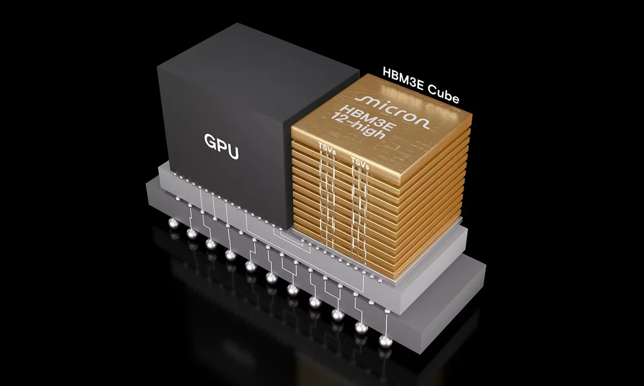
HBM means High Bandwidth Memory, whereas HBM3E is the latest and advanced type of RAM technology used explicitly in AI chips, data center chips, and applications in supercomputing.
Samsung 12-layer high-capacity HBM3E chips now allow approximately 50 percent storage increase and real bandwidth at over 1 TB/sec. This gracefully amplifies throughput many times toward the performance of GPUs or AI processors.
Nvidia and Samsung Coalition
All along, it has been working with HBM3E power fabricated by such firms as SK Hynix and Micron. The very first chip was created with 12-layer stacking technology, and that history is written down as an extremely monumental hallmark proudly held by Samsung and on its path into the next-generation AI processor of Nvidia-either the B100 or B200 series.
From its vantage point, it is strategic, enabling Nvidia to float production based on market demands through its multi-supplied memory to obviate some shortages.

As Far As The Future Goes
Not only does this event boost Samsung's technological credentials, but it also provides a huge stride toward an AI-paved tomorrow. Hence, a 12-layer HBM3E chip clears the path for denser, more energy-efficient, and high-performance AI solutions.
Were this to be credited, it would be a huge plus for AI developers, server companies, and HPC establishments.
You can also read: AMD Launches Zen 5 Pro Ryzen AI CPUs: All You Need to Know
Follow our WhatsApp channel for the latest news and updates